 |
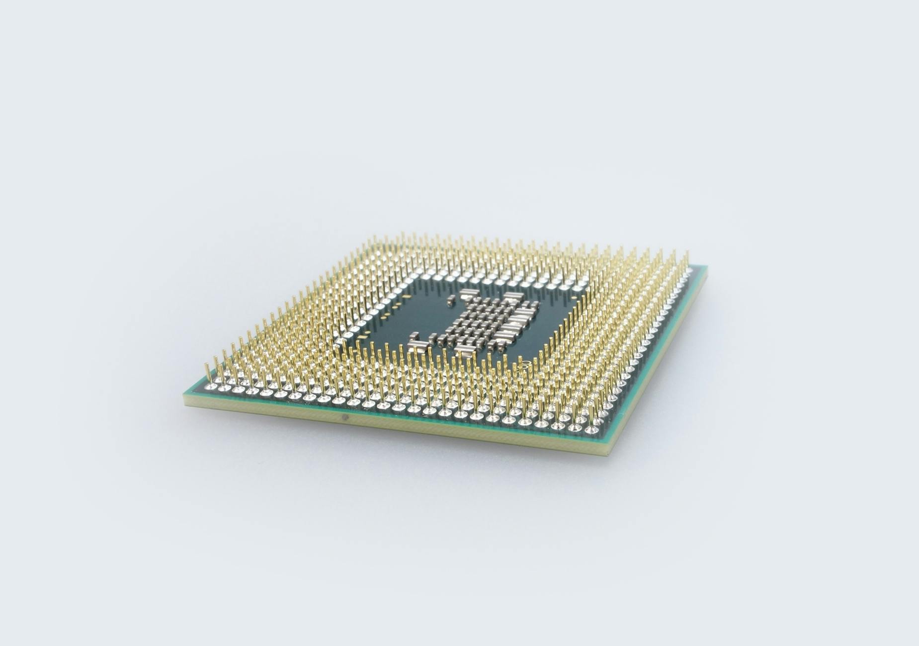
| AI Chip |
The semiconductor industry operates at the absolute outer boundaries of physical engineering. As chip architectures shrink into sub-2-nanometer dimensions, traditional manufacturing techniques face immense optical and thermodynamic hurdles. To overcome these barriers, chipmakers rely heavily on mathematical simulations known as computational lithography to print intricate circuit patterns onto silicon wafers.
In a major technical breakthrough, Siemens and NVIDIA have demonstrated a 12-fold speedup in AI chip lithography processes. By combining specialized Electronic Design Automation software with high-performance GPU acceleration, this partnership significantly reduces the time required to perform critical lithography simulations. This advancement comes at a crucial moment when the global semiconductor supply chain is under intense pressure to deliver next-generation artificial intelligence hardware faster and more efficiently.
Understanding Computational Lithography in Semiconductor Manufacturing
To appreciate the significance of a 12x speedup, it is essential to understand the underlying mechanics of photolithography. In modern semiconductor fabrication, light is shone through a photomask to print microscopic circuit features onto a light-sensitive chemical layer on a silicon wafer. However, because modern chip features are significantly smaller than the wavelength of light used to print them, extreme optical diffraction occurs.
Without correction, light waves bend and blur, causing printed transistors to warp, merge, or fail completely. Semiconductor engineers solve this using computational lithography—a suite of intensive mathematical algorithms that alter the shape of the photomask beforehand so that the final light pattern on the wafer is perfectly sharp.
The Core Components of Computational Lithography
- Optical Proximity Correction (OPC): Modifies mask geometry by adding micro-features like serif corners and line shifts to compensate for light diffraction.
- Inverse Lithography Technology (ILT): Uses inverse mathematical formulas to calculate the mathematically ideal photomask needed for precise target pattern generation.
- Source-Mask Optimization (SMO): Simultaneously optimizes both the illumination scanner light source and the photomask design to maximize process margins.
- Process Window Modeling: Simulates optical and chemical variations across millions of manufacturing conditions to ensure high wafer yield.
While effective, computational lithography is historically one of the most resource-intensive steps in chip design. Generating a single photomask set for an advanced node can require millions of CPU computing hours, consuming massive data center space and vast amounts of electrical power.
Deconstructing the Siemens and NVIDIA 12x Speedup
The strategic collaboration between Siemens and NVIDIA targets this computational bottleneck directly. By porting complex Electronic Design Automation (EDA) lithography algorithms from legacy CPU server architectures onto GPU-accelerated computing stacks, the combined system processes photomask calculations up to 12 times faster.
Confirmed reports highlight that this performance jump transforms computational lithography from a process that typically takes days or weeks down to just hours. This exponential gain is driven by parallel mathematical processing, where thousands of GPU cores execute wave-optics calculations concurrently across large layout windows.
Confirmed Technical Facts vs. Industry Analysis
To maintain absolute transparency, it is helpful to clearly separate confirmed factual details from broader technical analysis:
- Confirmed Fact: Siemens and NVIDIA have successfully demonstrated a 12x acceleration in lithography processing workloads for AI chips.
- Confirmed Fact: The implementation leverages hardware and software acceleration technologies optimized for EDA workflows.
- Technical Analysis: The 12x performance boost is expected to drastically lower the operational energy consumption of semiconductor fabs, as GPU clusters deliver vastly higher throughput per watt compared to legacy CPU-only data centers.
- Technical Analysis: Fabs utilizing this acceleration pipeline will likely shorten design tape-out turnaround times, enabling chip designers to iterate complex AI silicon layouts much more frequently.
For additional context on broader global manufacturing dynamics and technology trends, you can read our Semiconductor News Roundup, which details geopolitical shifts and technical innovations across leading chip foundries.
Real-World Industrial Use Cases and Applications
The 12x acceleration in lithography calculations delivers concrete advantages across multiple stages of semiconductor design and manufacturing pipelines.
1. Accelerated Time-to-Market for Custom AI Accelerators
Designing cutting-edge AI accelerators—including GPUs, Neural Processing Units (NPUs), and specialized Application-Specific Integrated Circuits (ASICs)—requires immense photomask complexity. With a 12x reduction in computational lithography processing time, fab engineering teams can run full-chip OPC runs overnight rather than waiting multiple weeks. This allows rapid verification of design rule changes and speeds up product launches.
2. High-NA EUV Lithography Integration
As the industry transitions to High-Numerical Aperture Extreme Ultraviolet (High-NA EUV) lithography machines, optical distortion models become exponentially complex. High-NA EUV systems introduce anamorphic magnification, requiring sophisticated mathematical adjustments across x and y axes. GPU-accelerated algorithms make complex Inverse Lithography Technology (ILT) mathematically practical for full-chip High-NA EUV mask generation.
3. Yield Optimization and Defect Mitigation
In high-volume silicon manufacturing, small physical variations can destroy chip yields. Fast computational lithography allows software engines to run broader stochastic simulations, analyzing how laser light interacts with photoresist chemicals across millions of scenarios. Identifying printability risks prior to physical mask creation directly improves fab yield rates.
Understanding structural shifts in specialized technology management requires robust engineering strategies, similar to organizational frameworks discussed in our BIM Initiates New Software and Technology Development Subsidiary: Strategic Analysis.
Key Benefits for Foundries and Chip Designers
The practical benefits of combining Siemens software capabilities with NVIDIA GPU platforms extend beyond simple computation speed. Fabs and fabless chip design firms gain structural advantages across economic and operational metrics.
- Dramatic Reduction in Data Center Footprint: Replacing thousands of CPU nodes with concentrated GPU acceleration racks drastically reduces the physical space required for computational mask synthesis.
- Reduced Operational Energy Consumption: Higher computational efficiency means lower power consumption per calculated mask layer, supporting corporate sustainability goals.
- Expanded Use of Full-Chip Inverse Lithography: Historically, full-chip ILT was limited due to compute costs. A 12x speedup makes full-chip ILT economically viable for standard production runs.
- Enhanced Iteration Speed for Engineering Teams: Physical design teams can fix design-rule check errors and re-simulate optical patterns rapidly without derailing launch schedules.
Limitations, Operational Risks, and Challenges
Despite the remarkable efficiency gains promised by a 12x speedup, industrial integration comes with practical limitations and strategic challenges that semiconductor companies must manage.
Hardware Dependency and Infrastructure Costs
Transitioning computational lithography workloads to GPU acceleration requires initial capital investment in enterprise GPU clusters, advanced networking hardware, and specialized storage infrastructure. Foundries must evaluate the capital expenditure (CapEx) against long-term operational savings (OpEx).
Legacy Software Integration
Electronic Design Automation codebases often contain decades of optimized x86 CPU routines. Porting legacy software algorithms to modern parallel computing frameworks like NVIDIA CUDA without introducing precision loss requires rigorous engineering effort and comprehensive quality assurance testing.
Supply Chain and Geopolitical Pressures
High-end hardware and advanced lithography software are subject to tight international export controls and trade regulations. Dependence on cutting-edge compute platforms means chipmakers must navigate potential supply constraints for hardware accelerators.
Future Outlook: The Road Ahead for AI Chip Lithography
The collaboration between Siemens and NVIDIA highlights a key technological trend: the convergence of artificial intelligence, high-performance computing, and physical manufacturing processes. Looking ahead, several key developments are set to shape the future of lithography:
- Generative AI in Mask Design: Beyond accelerating existing deterministic algorithms, researchers are exploring neural network models that can predict optical diffraction patterns in real time.
- Integration with Fabrication Digital Twins: Combining GPU-accelerated computational lithography with real-time digital twins of photolithography scanners will enable adaptive run-to-run control in semiconductor cleanrooms.
- Scaling Toward Sub-1nm Nodes: As atomic-scale effects become dominant, software simulation will be the main driver enabling physical silicon scaling.
Conclusion
The 12x speedup in AI chip lithography achieved by Siemens and NVIDIA is a major milestone in semiconductor manufacturing. By overcoming the massive compute bottlenecks inherent in optical proximity correction and inverse lithography, this technology enables faster iteration, lower energy consumption, and higher production efficiency for next-generation silicon.
As physical scaling approaches sub-2-nanometer regimes, GPU-accelerated computational tools will remain fundamental to sustaining technological progress across the entire electronics ecosystem.
Frequently Asked Questions (FAQ)
What is computational lithography in simple terms?
Computational lithography is a set of software simulations and mathematical algorithms used in chip manufacturing to alter photomask designs. It compensates for light bending and diffraction so that circuit patterns print accurately on silicon wafers.
How do Siemens and NVIDIA achieve a 12x speedup in lithography?
They achieved the 12x acceleration by optimizing Electronic Design Automation (EDA) software algorithms—such as Siemens Calibre lithography tools—to run on highly parallelized NVIDIA GPU computing platforms instead of traditional CPU-only server clusters.
Why is computational lithography critical for AI chips?
AI chips feature dense transistor layouts and massive interconnect architectures. Printing these complex sub-2-nanometer features requires extreme mathematical adjustments on photomasks, making fast computational lithography critical to ensuring functional chips and viable manufacturing yields.
Does this speedup reduce chip manufacturing costs?
Yes. By accelerating computation times from weeks to hours, fabs can lower data center power consumption, optimize capital equipment usage, reduce mask synthesis delays, and improve overall operational efficiency.
Will GPU acceleration replace CPU compute in semiconductor design completely?
While GPUs excel at massively parallel mathematical simulations like computational lithography, CPUs remain essential for sequential design tasks, data control flows, and management operations. Future EDA workflows will rely on hybrid architectures combining both CPU and GPU computing power.